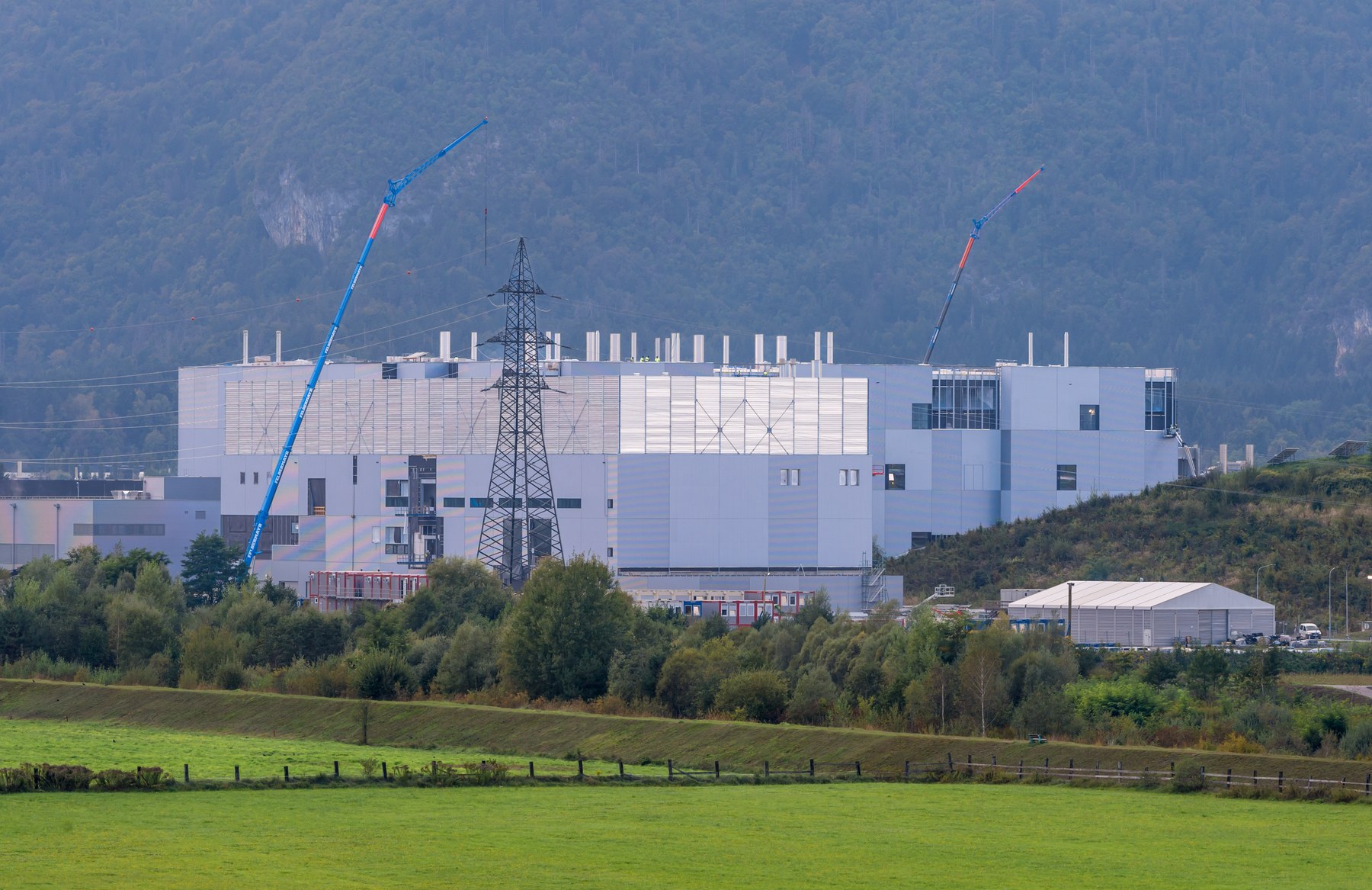
Infineon Technologies AG processed 300mm silicon carbide wafers into functional power devices at its fab in Villach, Austria. The company used existing silicon manufacturing equipment for the work. Infineon said a 300mm wafer can yield 2.3 times as many chips as a 200mm wafer.
What it means
Infineon plans to coordinate its 300mm SiC technology and production ramp with customers and partners while continuing its 200mm SiC manufacturing roadmap. The company also demonstrated Cold Split technology with 300mm SiC at its Dresden, Germany, site. Cold Split separates wafers from a silicon carbide boule with less material loss and shorter processing time than conventional wire sawing.
Infineon will display a processed 300mm SiC wafer at electronica 2026 in Munich from Nov. 10 to 13. The company will present in Hall C3, Booth 502.
Key facts
- Infineon processed 300mm silicon carbide wafers into functional power devices in Villach, Austria.
- A 300mm wafer provides 2.3 times more chips than a 200mm wafer, according to Infineon.
- Infineon is continuing its 200mm SiC manufacturing roadmap.
- Cold Split technology was demonstrated with 300mm SiC in Dresden, Germany.
- Infineon manufactures semiconductors using silicon, silicon carbide and gallium nitride.
- electronica 2026 runs Nov. 10 to 13 in Munich; Infineon will be in Hall C3, Booth 502.
Source: Infineon Technologies AG announcement