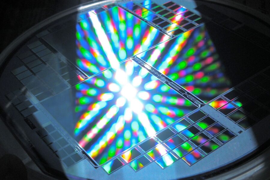

Applied Materials announced Oct. 12 that it opened its Equipment and Process Innovation and Commercialization Center, or EPIC Center, at its Sunnyvale, California, campus. The 600,000-square-foot semiconductor facility includes nearly four acres of advanced cleanroom space, and Applied Materials said capital spending on the center is expected to reach $5 billion.
What it means
The EPIC Center brings chipmakers, systems companies, equipment partners and research universities together to develop advanced chipmaking processes and move technologies from early research into high-volume manufacturing. Applied Materials said the facility combines materials, equipment and chipmaking work in one location.
TSMC, Intel, SK Hynix, Micron, Samsung Electronics, Broadcom and Advantest are listed as industry partners. Arizona State University, Stanford University and the University of California, Berkeley are university partners. Applied Materials also partnered with SK Hynix to accelerate memory innovation.
Key facts
- Applied Materials announced the EPIC Center on Oct. 12 at its Sunnyvale, California, campus.
- The facility covers 600,000 square feet.
- The center includes nearly four acres of advanced cleanroom space.
- Applied Materials expects $5 billion in capital spending on the center.
- Applied Materials reported $7.01 billion in Q1 revenue.
- The company cited demand for leading-edge logic, high-bandwidth memory and advanced packaging.
Source: Manufacturing Dive, reporting an Applied Materials announcement